Ion Implantation Consumables and Repair Parts for Applied Materials® / AMAT® Implanters
Glemco is a Turnkey Solution for Semiconductor Wafer Manufacturers
We carry stock of high use ion implantation consumables, manage in site inventory, customize kitting or labeling.
We have a broad, high quality product line of ion implantation consumables for the entire beamline, full of innovative solutions.
We perform refurbishments and repairs of assemblies critical to ion implantation.
We provide experienced technical support and the best customer service experience.
Ion Implantation consumables and machine maintenance and support for 9000/9200™, 9500™, Quantum™, XR80™, XR LEAP™
Applied’s portfolio comprises the four types of implant systems common in the industry. Three of these are line-of-sight beam line systems: high-current (for low-energy and/or high-dose applications); medium-current (for lower doses); high-energy (for very deep implants). The fourth uses plasma doping for applications requiring exceptionally high doses or conformal doping of regions that cannot be reached with the line-of-sight beam line systems (e.g., sidewall doping in three-dimensional fin field effect transistors). These systems deliver leading-edge beam angle control, dose control, uniformity, and wafer-to-wafer repeatability.
Moving Clips and Fixed Restraints for AMAT End Stations
Applied Quantum™
Quantum™ LEAP(tm) (Low Energy Advanced Processing) ion implantation systems were introduced in July 1999. The Quantum™ ion implantation system uses a new, small footprint platform that bridges 200mm and 300mm wafer sizes. High throughput and productivity are possible at low energies down to 200eV — a requirement for the critical implants used in 0.18 micron and below devices.
The Quantum™ system’s extremely short beam path minimizes beam “blow up” and energy contamination, with new technology that ensures energy accuracy and control for ultra-low energy implants to +/-0.5%. Quantum™ implanters are currently available in three models: the Quantum™ LEAP technology, which offers an ultra-low energy range of 200eV to 80keV; the Quantum™ 80, which covers a range of 2keV to 80keV; and the Quantum™ 120, which performs at an extended upper energy range to 120keV.
Quantum™ xR80 and xR LEAP’s System of low energy implantation is an essential technology for the fabrication of semiconductors using 0.18 micron and below features. Designed for 300mm wafers, the Quantum™ evolutionary platform is easily adaptable to 200mm and 150mm wafer sizes. The system incorporates a 300mm compatible factory automation module for fully automatic wafer handling, yet remains almost the same size as the company’s compact 200mm xR LEAP system.
Maximum 200mm mechanical throughput range has been extended from the xR LEAP to doses of 1E15, while the system achieves a 60 percent throughput increase when used for quad implants. Quantum™‘s extremely short source-to-wafer beam path, which minimizes beam “blow up” and energy contamination, has been further optimized to improve precision at all energies. New technology ensures excellent energy accuracy and improved energy control for ultra-low energy implants to a remarkable +/- 7.5 volts.
The xR80 was the first implanter to successfully address low energy boron, and the xR LEAP was the first sub-keV implanter.
Applied Materials® RTP (rapid thermal processing) Centura system created the industry’s first integrated, high-performance, ultra-shallow junction (USJ) module, making it possible for chipmakers to reliably form the complex junctions needed for next-generation devices. Quantum™ extends the capabilities of the USJ module even further, enabling significant gains in productivity.
The Quantum™ LEAP for ultra-low energies offers a range of 200eV to 80keV enables implant of ultra shallow junctions in the most advanced devices.
The Quantum™ 80 offers a range of 2keV to 80keV, covering virtually all of the high current implants used in 0.25 micron to 0.18 micron designs.
For customers requiring an extended upper energy range, the Quantum™ 120 boosts energy to 120keV.
Applied Quantum™ III is a batch implanter which elevates low energy implant performance to levels never before achieved in the industry. The Quantum™ III system breaks the 50 wafer-per-hour throughput barrier for critical 90nm-generation low energy implants by increasing beam current 15-20 percent for most applications, while significantly reducing scan time, to provide a 20-50 percent gain in system productivity
The Applied Quantum™ III system features a number of proven technology and productivity enhancements that provide customers with increased process control and throughput for traditionally difficult and time-consuming implant applications. Design improvements in the Quantum™ III system’s low-energy beamline allow faster and more accurate doping of source/drain and gate structures.
The Quantum™ III system provides chipmakers with the extendibility to perform high-accuracy ultra-shallow junction implants for 90nm and below designs.
The Quantum™ line has achieved distinction by enabling a full range of low-energy and high-current implant applications with high productivity, providing chipmakers with a flexible and cost-effective solution that is extendible to 0.1 micron geometries and 300mm wafers.
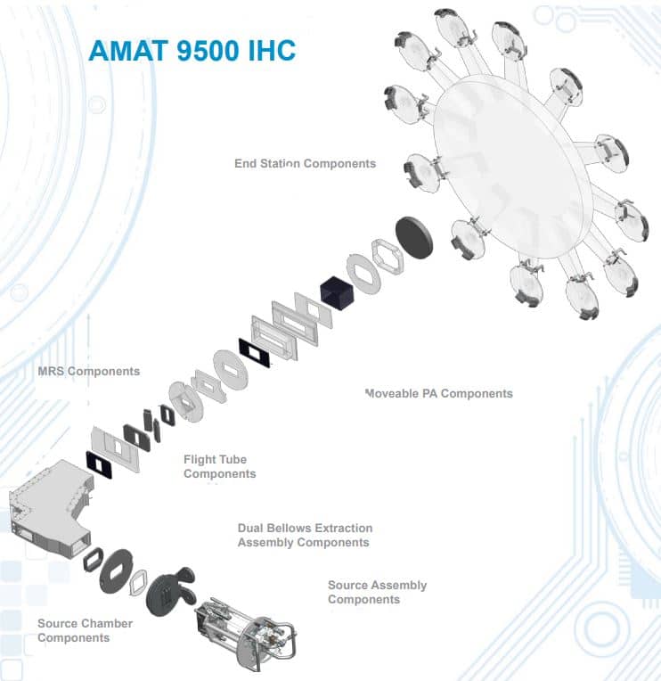
AMAT® / APPLIED MATERIALS® 9500sup>™ is an ion implanter and monitor device that is made for various semiconductor manufacturing needs. It is a high-performance device, with a two-axis vacuum and modular chamber system, that enables users to process large-scale devices with greater efficiency and accuracy. It also includes a dynamic ionization void reduction system that reduces particle contamination while maintaining excellent implant and monitor performance.
AMAT® 9500sup>™ components have been designed to meet the highest standards in processing and monitoring, ensuring the highest quality of electronic device manufacturing. The device has a proven track record of delivering stable processing, even during complex processes such as rapid thermal annealing and rapid pulse injection. It features an ion guide with a linear design that allows for exceptionally accurate and stable particle trajectories, reducing the potential for damage to the substrate. It also utilizes an automatic wafer rotation feature that enables operators to precisely align the wafer before processing.
APPLIED MATERIALS® 9500sup>™ is also equipped with innovative software that significantly increases monitoring and maintenance functionality. This includes a powerful diagnostics system for obtaining analytical feedback about the machine’s performance. This helps users determine areas in need of improvement. Thanks to its optimized design, 9500sup>™ is capable of performing a variety of implantation and monitoring tasks, including diffusion, oxidation, and deposition. It is also capable of producing high ion doses and controlling ion beam energy to achieve the desired implantation result. This makes AMAT® / APPLIED MATERIALS® 9500sup>™ an excellent choice for various applications, ranging from intricate design processes to high-volume production lines. Overall, AMAT® 9500sup>™ is a high-performance, efficient, and reliable ion implanter and monitor device that is ideal for a wide range of semiconductor manufacturing applications. Its optimized design and advanced features make it an excellent choice for the demanding production needs of today’s electronic device manufacturers.
Gallery
Since 1984
We are proud to support our local communities with jobs that offer good working environment, excellent pay and benefits, growth opportunities and stability. Proud to be an American Manufacturer and a Woman Owned Business.
Contact Us Today
