The Process of Ion Implantation
Ion implantation is a key process in the semiconductor industry used to introduce impurities into silicon wafers to modify their electrical properties. These machines are designed to provide precise and controlled implantation of ions into the wafer, high throughput, improved process control, and excellent uniformity. They are used for a wide range of applications, including logic, memory, and power devices.
Ion implantation can see temperatures up to 1400 C, and the aggressive nature of the process require significant heat resistance. Components and spare parts for these systems are made from refractory metals such as Molybdenum, Tungsten, and Tantalum or from other materials that offer corrosion resistance, ability to withstand high temps and good thermal conductivity, like graphite, ceramic, and engineered performance plastics. It is important to use pure metals, and to pay attention to form, fit, and function and precision geometries.
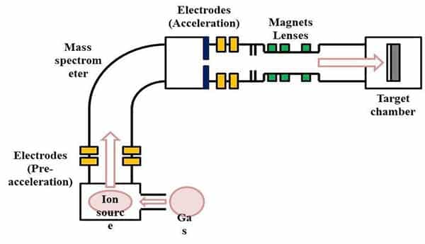
Ion implantation is a materials engineering process by which ions of a material are accelerated in an electrical field and directed into the wafer, typically to form the source and drain regions of the transistor.
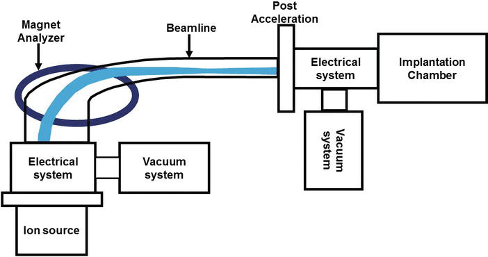
Ion implantation equipment typically consists of an ion source, where ions of the desired element are produced, an accelerator, where the ions are electrostatically accelerated to a high energy, and a target chamber, where the ions impinge on a target, which is the material to be implanted. Thus ion implantation is a special case of particle radiation. Each ion is typically a single atom or molecule, and thus the actual amount of material implanted in the target is the integral over time of the ion current. This amount is called the dose. The currents supplied by implanters are typically small (microamperes), and thus the dose which can be implanted in a reasonable amount of time is small. Therefore, ion implantation finds application in cases where the amount of chemical change required is small.
Glemco supports ion implantation as a manufacturer of high quality Ion Implantation consumables, as well as repair and maintenance parts.
Ion Energies & Accelerator Systems
Typical ion energies are in the range of 10 to 500 keV (1,600 to 80,000 aJ). Energies in the range 1 to 10 keV (160 to 1,600 aJ) can be used, but result in a penetration of only a few nanometers or less. Energies lower than this result in very little damage to the target, and fall under the designation ion beam deposition. Higher energies can also be used: accelerators capable of 5 MeV are common. However, there is often great structural damage to the target, and because the depth distribution is broad, the net composition change at any point in the target will be small.
The energy of the ions, as well as the ion species and the composition of the target determine the depth of penetration of the ions in the solid: A monoenergetic ion beam will generally have a broad depth distribution. The average penetration depth is called the range of the ions. Under typical circumstances ion ranges will be between 10 nanometers and 1 micrometer.
Accelerator systems for ion implantation are generally classified into medium current (ion beam currents between 10 μA and ~2 mA), high current (ion beam currents up to ~30 mA), high energy (ion energies above 200 keV and up to 10 MeV), and very high dose (efficient implant of dose greater than 1016 ions/cm2).
Dopant ions such as boron, phosphorus or arsenic are generally created from a gas source, so that the purity of the source can be very high.
One prominent method for preparing silicon on insulator (SOI) substrates from conventional silicon substrates is the SIMOX (separation by implantation of oxygen) process, wherein a buried high dose oxygen implant is converted to silicon oxide by a high temperature annealing process.
Suppliers of ion implanters include Applied Materials®/Varian®, and Axcelis®
Since 1984
We are proud to support our local communities with jobs that offer good working environment, excellent pay and benefits, growth opportunities and stability. Proud to be an American Manufacturer and a Woman Owned Business.
Contact Us Today