Full-Service Supplier for the Semiconductor Industry
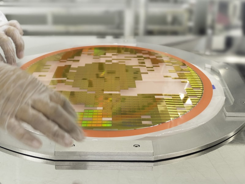
Integrated Circuit manufacturing is the midstream of the semiconductor industry, where the fab or foundry must transfer the designed circuit diagram to the semiconductor wafer. We support the industry with our own product line of ion implantation consumables, as well as CVD, abatement, lithography and epitaxy processes with high quality consumables, money-saving refurbishments and rebuilds, new or customized assemblies, and unique solutions.
Silicon wafer processing relies on the use of ion implantation systems which inject ions at high energy directly into silicon wafer surfaces. The ion plasma source is energized via refractory metal electrodes which operate within fabricated molybdenum or tungsten arc chambers. Tantalum is used occasionally in the Ion source but is less common.
Glemco specializes in materials used specifically in the semiconductor industry, manufacturing parts for the entire beam line: end station, electron scanning, magnetic quadrapole, ion acceleration, mass analyzer, Magnet Chamber, filament cathode, and ion source. We have an extensive line of graphite product for the beamline, source, electrodes, extraction asemblies, faraday and post Accel. We manufacture parts for plasma etch equipment chambers, like gas trench covers for CVD and HDP equipment. We manufacture assemblies for APCVD like the nitrogen shield and spider tubes. We can provide new or repair/refurbish assemblies like Source Assemblies and Vaporizers, Manipulator Assemblies Electrode Assemblies for the implanter, the Pneumatic Actuator for KLA-SEM, IVAs for APCVD, the RF Coil Assembly and the RF Cone assembly for the Resonator, or moving clip assemblies for AMAT end stations.
Glemco is your premier solution for legacy semiconductor equipment support as the OEMs discontinue support of equipment like Legacy Axcelis GSD implanters and Legacy Viista, Viision, and Quantum AMAT implanters
We carry stock of high use ion implantation consumables for legacy equipment.
Our Semiconductor Expertise
Glemco specializes in these refractory metal products that are extraordinarily resistant to heat and wear. All refractories share some properties, including a melting point above 2000 °C and high hardness at room temperature. They are chemically inert and have a relatively high density.
Other materials commonly used in the semiconductor industry are aluminum, boron nitride, stainless steels, alumina, copper and copper alloys, engineered plastics, high purity nickel and nickel alloys like Hastelloy and Inconel, and graphite.
Graphite is a critical material use in the semiconductor industry. A neutral material that is easily filtered out of the beam, it can withstand the extreme plasma environment of the implantation process. Graphite is often involved directly in the beam path where contamination can ruin millions of dollars in chips extremely quickly; it’s essential that the graphite used in this process is very clean. All graphite product manufactured by Glemco is certified contaminant free to <5ppm.
Semiconductor equipment that has been in use for years is still active and requires support. Our catalog of product encompasses the entire lifetime of the semiconductor industry. Our longevity in this industry means we intimately understand what it is we are making, how it all works together, and what is critical.
The industry is constantly innovating to meet the demands of today’s chip market. Utilizing older equipment for today’s marvelous technology requires changes. Glemco supports innovation in the semiconductor industry with performance upgrades and modifications and repair services that can extend the life of critical parts and assemblies.
As a full-service supplier to the semiconductor industry, we carry frequently ordered items in stock, offer inventory management, custom kitting, custom labeling, and will make every attempt to accommodate expedite requests.
Since 1984
We are proud to support our local communities with jobs that offer good working environment, excellent pay and benefits, growth opportunities and stability. Proud to be an American Manufacturer and a Woman Owned Business.
Contact Us Today